Gatan Digital Camera

EELS & EFTEM Systems GIF Quantum Energy FiltersHigh throughput spectrometers to capture highly detailed data from your EELS and EFTEM experiments. Enfinium SpectrometersDedicated, hard-working spectrometers for your EELS experiments. GIF Quantum LS Imaging FilterMaximize your resolution and contrast for cryo-EM by combining low distortion GIF Quantum optics with a K2 Summit detector that offers a “frame rate 10x higher than other[s]” and produces “a DQE as high as 80%.” K2 IS CameraHighest performance in-situ camera to resolve dynamic details in heating, catalysis, mechanical deformation, STEM diffraction, electrical testing, and chemical reaction experiments. K2 Direct Detection CamerasCryo-EM – Nature’s 2015 Method of the Year – is being led by the K2 camera that offers a "frame rate 10x higher than other detector brands” and produces “a DQE as high as 80%.” OneView CameraWinner of the 2015 Microscopy Today Innovation Award. The ONE camera to capture 16 MP images and video in all your TEM applications.
Orius CamerasFiber-optically coupled CCD camera ideal for applications that require high sensitivity and pixel resolution. UltraScan CameraReliable workhorse that delivers high-speed acquisition, with applications ranging from sub-angstrom HREM to in-situ transmission electron microscopy, from electron diffraction to low dose cryo-electron microscopy. Vulcan Cathodoluminescence DetectorGain insight into your sample’s optical and electronic properties.
Used Prom Dresses Bend Oregon Advanced STEM DetectorsHigh-angle annular dark field (HAADF), annular dark field (ADF) plus bright and dark field (BF/DF) detectors for STEM imaging optimized for electron energy loss spectroscopy (EELS).
Briggs Toilet Bowl STEMPack Spectrum ImagingA powerful method of obtaining detailed analytic data from a sample on an electron microscope equipped with scanning mode.
50tree T Shirt
In-Situ Video SoftwareSynchronize your images with data from in-situ devices. TEM AutoTune SoftwareAutomates adjustment of focus, astigmatism, and misalignment. DigitalMontage SoftwareStage and optics control so you can seamlessly stitch images together. HREM AutoTune SoftwareFacilitate your HREM assays by automatically adjusting the critical imaging parameters of a TEM microscope focus, stigmation, and beam tilt. DIFPACK ModuleDiffraction analysis package (DIFPACK) to automate the selection area of your electron diffraction (SAED) patterns and high resolution lattice images of crystalline samples. HoloWorks SoftwareEnables Fourier optics simulation and simplifies off-axis hologram processing. 3D Tomography Acquisition SoftwareSupports your tomographic tilt series acquisition experiments using TEM, STEM, or EFTEM modes. EELS, EFTEM & STEM Software EELS AdvisorSimulation tool to eliminate the guesswork from your EELS and EFTEM compositional mapping experiments.

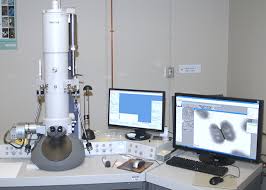
Advanced AutoFilter SuiteAutomates your multi-element EELS and EFTEM data acquisition experiments. GIF Tridiem 863 Upgrade to Gatan Microscopy Suite 2AutoFilter palette streamlines all steps from filter alignment through data acquisition.Philips / FEI (Morgagni) Transmission Electron Microscope with Gatan Digital Camera Philips / FEI (Morgagni) Transmission Electron Microscope with Gatan Digital Image acquisition is by a CCD camera and microscope control occurs through the Morgagni user interface and integrated image analysis software. Image analysis and enhancement may be done immediately after image capture. Maximum magnification for most samples is 110,000X. Home / Products / TEM Imaging & Spectroscopy / Most flexible range of applications including materials science, in-situ, biological, and diffraction covered by the Orius family of cameras Fast frame rate with binning allows real-time setup and microscope optimization without viewing screen

True transmission scintillator (Orius 833) offers best-in-class diffraction performance without worrying about damage Cameras are available both for bottom mount or 35 mm port locations for high resolution or high field of view applications Duty cycle (in view mode) On-axis or 35 mm port (retractable) 35 mm port (retractable) On-chip (100x full well) Full well (CCD e-) 1 ms to 100 s IEEE 1394b (Firewire 800) IEC 61010-1: Third editionTEM imaging with Gatan digital camera Graphite lattice spacing of 0.335 nm Carbon black Gold nano particles on carbon film Crystal lattice of rutile Ni nanoparticles with cabon coating Palladium nanoparticles on carbon support Lung epithelial cell Spores of C. difficile bacteria

Home / Techniques / There are a number of options and technologies available for digital imaging in transmission electron microscopy (TEM) applications today. Traditionally, high energy electrons could not be directly exposed to a sensor without excessively damaging the detector. As a consequence, conventional TEM cameras first expose the incoming electron beam to a scintillating film that converts the electrons into light (photons). These photons are then transferred to the sensor, either through a series of optical lenses or a coupled fiber optic plate. Finally, the light is collected by a sensor where the image is created pixel-by-pixel based on the amount of light detected at each position in the sensor. Conventional TEM image detection architecture There are four basic steps in TEM imaging to address incoming electrons: Convert electrons to signal Detect signal with sensor Electronically transfer signal and read-out to form image What is different with direct detection?

There are only two steps in TEM imaging with direct detection: Convert electrons to signal – not applicable One key difference between conventional and direct detection is a custom CMOS sensor that utilizes the only radiation hard architecture that can tolerate direct exposure to high energy particles. To add, extremely high speed electronics for data transfer and processing enable low-dose counting and super-resolution capabilities. Combined, this allows frame rates (4k x 4k) of 400 frames per second (fps) to be processed in real-time to achieve optimal results. Convert electrons to signal Transfer signal Detect signal with sensor Transfer signal and read-out image Step 1) Convert electrons to signal Gatan uses proprietary phosphor scintillators to optimize signal conversion that enhances detector sensitivity (SENS) and resolution. When you select a scintillator, it is appropriate to know the performance trade-offs between SENS and resolution.

Sensitivity (signal): Ideal for dose-sensitive use cases where you need to generate more photons per incoming electron (e.g., cryo-tomography, beam sensitive materials) Resolution (spatial detail): Favorable for applications where you require more information to resolve details, but you can increase the dose (signal) without harming the sample (e.g., semiconductors and other less-sensitive materials) Step 2) Transfer signal Various coupling (lens- and fiber-coupled) mechanisms are available to optimize signal transfer and meet cost or performance targets for a given detector. Lens-coupled: Lens optics transmit light to the sensor where it is converted into sensor electrons (signal) Pros: (Gatan) Uses real transmission scintillator; can be less expensive than higher performance fibers Cons: Light (information) loss with lensing, angular dependencies (<10% efficient); vignetting (light fall-off); image distortion for higher magnification Fiber-coupled: Scintillator creates photons that subsequently create sensor electrons; fiber directly transmits light to sensor with high efficiency Pros: Most efficient transmission of light information to the sensor (1:1 coupling of scintillator:sensor (>50% efficient) with no image distortion);

can trade-off SENS verses resolution (fiber configuration detail) Cons: Fiber optics are slightly higher cost; requires process optimization including cladding, sintering, bonding of fibers (Gatan proprietary) Step 3) Detect signal with sensor Sensor type (CCD vs. CMOS) offers significant trade-offs for TEM camera performance as there are fundamental differences in architecture. Charge-coupled device (CCD): Charge transfers between neighboring cells, and read-out (e.g., noise) is seen at final stage; binning minimizes the impact of read-out noise Complementary metal–oxide–semiconductor (CMOS): Charge immediately converts to voltage (read-out with digital output); supports high frame rates, low overall electronics noise Both technologies possess inherent advantages, so the question arises about what unique performance characteristics arise from each choice. CCDs can have 100% fill factor that captures all incoming light, whereas part of the CMOS sensor is occupied by transistors and metal wiring associated with each pixel.

Historically, CCDs provided higher quality images with low noise, at affordable prices. Recent design advancements and processing techniques now advance CMOS sensor performance so it is a viable choice for some applications. Note that CCDs still maintain an advantage for binning in terms of signal-to-noise. However, CMOS chips can scale the number of read-out ports and achieve very high frame rates. Step 4) Transfer signal and read-out image When a charge converts to voltage, you typically generate noise CCD: Transfer data out of serial register CMOS: Converts to voltage per pixel It is very important to optimize read-out noise (higher voltages) and speed (multi-port and fast read times) for CCDs. Optimize controller for low read-noise; leverage multi-port read-outs for faster speed Interline CCDs with binning have the fastest readouts (fps) – up to 30 fps due to 100% duty cycle CMOS typically is seen as a fast sensor because you can run in rolling shutter mode verses the slow global shutter mode.